
The global 3D IC and 2.5D IC packaging market is witnessing significant growth as semiconductor manufacturers increasingly adopt advanced packaging technologies to support artificial intelligence workloads, high-performance computing, automotive electronics, and next-generation consumer devices. Rising demand for AI accelerators, high-bandwidth memory (HBM), and compact high-performance semiconductor architectures is accelerating investment in advanced packaging infrastructure worldwide.
3D IC and 2.5D IC Packaging Market Snapshot
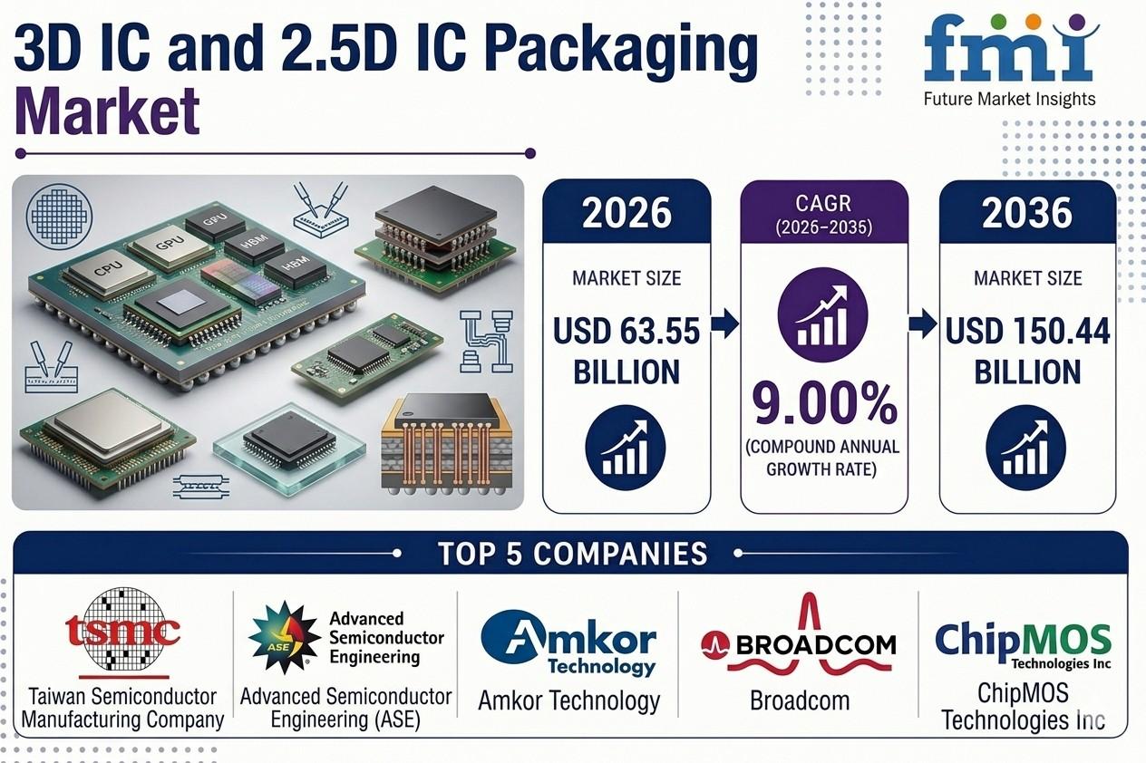
- Market Size (2026): USD 63.55 billion
- Forecast Market Size (2036): USD 150.44 billion
- Forecast CAGR (2026–2036): 9.0%
- Leading Technology Segment: 3D TSV (50.6% share)
- Leading Application Segment: Logic (45.9% share)
- Largest End-use Industry: Consumer Electronics (38.4% share)
- Fastest Growing Market: China (12.2% CAGR)
- Key Growth Drivers: AI accelerators, HBM memory, data centers, automotive electronics, and advanced computing
Get Detailed Market Forecasts, Competitive Benchmarking, and Pricing Trends: https://www.futuremarketinsights.com/reports/sample/rep-gb-25260
Market Overview
3D IC and 2.5D IC packaging technologies enable multiple semiconductor dies to be integrated into a single package using advanced interconnect architectures such as:
- Through-silicon vias (TSVs)
- Silicon interposers
- Wafer-level chip-scale packaging
- Heterogeneous die integration
These technologies provide major advantages including:
- Higher bandwidth
- Lower power consumption
- Reduced latency
- Compact form factors
- Improved thermal efficiency
The market is increasingly driven by the rapid expansion of AI infrastructure and advanced computing applications.
AI Accelerators Fueling Packaging Demand
Artificial intelligence workloads are becoming the largest growth catalyst for advanced semiconductor packaging.
Rising AI Chip Production
Leading AI chips including:
- NVIDIA H100 and B100 GPUs
- AMD MI300X accelerators
- Google TPU platforms
require advanced 2.5D packaging technologies such as:
- TSMC CoWoS
- Intel EMIB
- Silicon interposer architectures
These packaging solutions are essential for integrating high-bandwidth memory adjacent to logic processors.
Traditional 2D semiconductor packaging can no longer support the interconnect density and memory bandwidth requirements demanded by modern AI accelerators.
HBM Memory Driving TSV Adoption
3D TSV Technology Holds 50.6% Market Share
Through-silicon via (TSV) technology remains the dominant packaging technology because it enables vertical stacking of memory dies.
HBM manufacturers including:
- SK Hynix
- Samsung
- Micron
are increasingly deploying TSV stacking technologies to support:
- 8-high HBM stacks
- 12-high HBM4 memory architectures
Each AI accelerator package typically requires multiple HBM stacks, creating massive demand for advanced TSV packaging capacity.
Key Advantages of TSV Technology
- High-density vertical integration
- Reduced interconnect length
- Improved signal integrity
- Lower power consumption
- Higher bandwidth efficiency
Advancements in TSV manufacturing are also improving production yields and reducing overall packaging costs.
Logic Applications Dominate Market Demand
Logic Segment Accounts for 45.9% Share
Logic applications remain the leading segment due to rising demand for:
- AI processors
- High-performance CPUs
- GPUs
- Advanced microcontrollers
- Data center accelerators
Advanced packaging technologies allow logic chips to integrate memory and compute components within a single package, enabling:
- Faster data transfer
- Lower latency
- Enhanced power efficiency
- Reduced footprint
The increasing complexity of AI and cloud computing workloads continues accelerating demand for advanced logic packaging solutions.
Consumer Electronics Remain Largest End-use Sector
Consumer Electronics Hold 38.4% Market Share
Consumer electronics remain the largest end-use industry because of strong demand for compact and high-performance devices including:
- Smartphones
- Tablets
- Wearables
- Gaming consoles
- AR/VR devices
Electronics manufacturers increasingly rely on 3D and 2.5D packaging to deliver:
- Miniaturized designs
- Improved graphics performance
- Better battery efficiency
- Enhanced thermal management
As consumer expectations continue rising, advanced packaging is becoming a critical differentiator in device performance.
Automotive Electronics Emerging as Major Opportunity
The automotive sector is rapidly adopting advanced semiconductor packaging technologies for:
- ADAS systems
- Autonomous driving platforms
- Sensor fusion modules
- In-vehicle AI computing
Key Automotive Packaging Applications
Manufacturers are integrating:
- LiDAR processors
- Radar ASICs
- Vision processors
- AI compute modules
into advanced heterogeneous 2.5D packages.
These systems require:
- High computational performance
- Low power consumption
- Compact packaging
- Reliable thermal management
The growth of electric vehicles and autonomous driving technologies is expected to create substantial long-term opportunities for advanced packaging providers.
High-performance Computing Expanding Market Growth
The growth of cloud computing, AI data centers, and enterprise workloads is significantly increasing demand for advanced semiconductor packaging.
HPC and Data Center Requirements
Modern data centers require:
- High memory bandwidth
- Faster processing speeds
- Low latency interconnects
- Efficient thermal performance
Advanced 3D IC and 2.5D packaging technologies help address these requirements while improving energy efficiency and integration density.
Key Technology Trends
Smart Manufacturing and Automation
Semiconductor packaging manufacturers are increasingly deploying:
- AI-driven yield optimization
- Automated inspection systems
- Advanced thermal management solutions
- Precision assembly technologies
These innovations improve:
- Packaging reliability
- Manufacturing efficiency
- Production scalability
- Defect reduction
Heterogeneous Integration
The market is rapidly moving toward heterogeneous integration where multiple chip types are combined within a single package.
This includes integration of:
- Logic chips
- Memory dies
- Sensors
- Analog components
- Accelerators
Speak to Analyst: Customize insights for your Business Strategy: https://www.futuremarketinsights.com/customization-available/rep-gb-25260
Key Market Drivers
- Rising AI and Data Center Demand: AI accelerators and cloud infrastructure continue driving unprecedented demand for advanced packaging technologies.
- Growth in High-bandwidth Memory: HBM adoption in AI GPUs is accelerating TSV packaging demand globally.
- Miniaturization of Electronics: Compact consumer electronics require higher-density semiconductor integration.
- Automotive Automation: ADAS and autonomous driving platforms increasingly require advanced semiconductor packaging architectures.
Market Challenges
High Manufacturing Costs
Advanced packaging technologies require substantial investment in:
- TSV fabrication
- Silicon interposers
- Precision assembly
- Thermal management systems
Yield and Thermal Management Issues
Manufacturers continue facing challenges related to:
- TSV yield optimization
- Heat dissipation
- Packaging complexity
- Supply chain constraints
Competitive Landscape
The 3D IC and 2.5D IC packaging market remains highly competitive, led by major foundries, OSAT providers, and semiconductor companies.
Leading Companies
Key market players include:
- TSMC
- Intel Corporation
- Samsung Electronics
- ASE
- Amkor Technology
- Broadcom
- JCET
- SPIL
- PTI
- UMC
- Xilinx
Industry Focus Areas
Companies are investing heavily in:
- CoWoS expansion
- EMIB technologies
- HBM integration
- Advanced interposers
- AI packaging platforms
Future Outlook
The 3D IC and 2.5D IC packaging market is expected to witness sustained long-term growth driven by:
- AI accelerator expansion
- HBM memory demand
- Automotive semiconductor growth
- High-performance computing
- Advanced consumer electronics
Companies investing in:
- Advanced TSV technologies
- AI-focused packaging infrastructure
- Heterogeneous integration
- Thermal management innovations
- Next-generation HBM platforms
are expected to gain major competitive advantages during the forecast period.
Executive Summary
- 3D IC and 2.5D IC packaging market projected to reach USD 150.44 billion by 2036
- AI accelerators and HBM memory driving unprecedented advanced packaging demand
- 3D TSV technology dominates with 50.6% market share
- Logic applications remain the leading segment with 45.9% share
- Consumer electronics continue leading end-use demand
- Automotive and autonomous driving systems creating major new opportunities
- China remains the fastest-growing regional market globally
- AI infrastructure and high-performance computing will continue reshaping semiconductor packaging innovation
Read Full Report- https://www.futuremarketinsights.com/reports/3d-ic-and-25d-ic-packaging-market
Have a Look at Related Research Reports on the Packaging Domain:
Thin Wall Packaging Market: https://www.futuremarketinsights.com/reports/thin-wall-packaging-market
Mycelium Based Packaging Market: https://www.futuremarketinsights.com/reports/mycelium-based-packaging-market
EPS Shippers Market: https://www.futuremarketinsights.com/reports/eps-shippers-market
Contact Us:
Future Market Insights Inc.
Christiana Corporate, 200 Continental Drive,
Suite 401, Newark, Delaware - 19713, USA
T: +1-347-918-3531
For Sales Enquiries: sales@futuremarketinsights.com
Website: https://www.futuremarketinsights.com
About Future Market Insights (FMI)
Future Market Insights, Inc. (FMI) is an ESOMAR-certified, ISO 9001:2015 market research and consulting organization, trusted by Fortune 500 clients and global enterprises. With operations in the U.S., UK, India, and Dubai, FMI provides data-backed insights and strategic intelligence across 30+ industries and 1200 markets worldwide.