
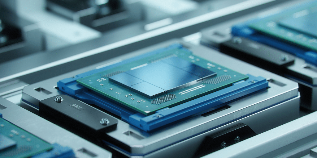
The advanced semiconductor packaging industry is witnessing significant transformation driven by the demand for miniaturization, enhanced performance, and integration capabilities in electronic devices. Increasing investments in semiconductor manufacturing technologies and the push for heterogeneous integration have positioned this market as a critical component in the semiconductor value chain.
Market Size and Overview
The Advanced Semiconductor Packaging Market is estimated to be valued at USD 41.61 Bn in 2025 and is expected to reach USD 72.24 Bn by 2032, growing at a compound annual growth rate (CAGR) of 8.2% from 2025 to 2032.
The growth in market size is propelled by accelerating adoption across consumer electronics, automotive, and telecommunications segments, with evolving Advanced Semiconductor Packaging Market Dynamics influenced by innovations in packaging architectures and materials.
Market Segments
The advanced semiconductor packaging market analysis reveals three core segments: packaging type, end-use industry, and technology category. Within packaging type, system-in-package (SiP) dominates due to its ability to support complex functionalities, while fan-out wafer-level packaging (FOWLP) shows the fastest growth, with a surge of 15% in market revenue during 2024-2025 attributed to enhanced signal integrity benefits.
In end-use industries, consumer electronics remains the dominant sub-segment, driven by smartphones and wearables, whereas automotive electronics is the fastest-growing segment, fueled by the rise of electric vehicles and ADAS applications. Technology-wise, through-silicon via (TSV) technology leads established methods, with emerging embedded die packaging rapidly gaining traction for its performance and space-saving advantages.
‣ Get more insights on : Advanced Semiconductor Packaging Market
‣ Get this Report in Japanese Language: 先端半導体パッケージ市場
‣ Get this Report in Korean Language: 첨단반도체패키징시장